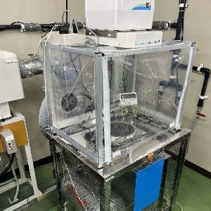
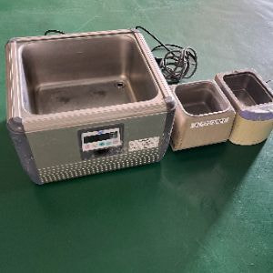
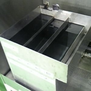
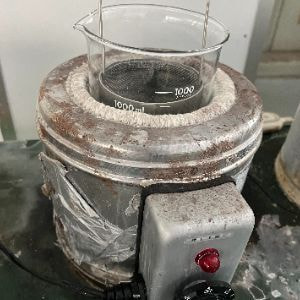
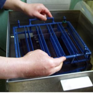
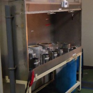
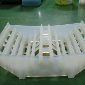
Process Flow(For example)

Subsidy Project for Strengthening the Semiconductor and Battery Industry Cluster in Yamaguchi Prefecture for FY 2024 (Promotion of Material Development, etc.)
We have researched and developed a technology for removing burrs generated when dicing substrates for semiconductors.
- We have researched, developed, and equipped a technology that accurately removes metal burrs from semiconductor microchips without damaging the chips.
- It is suitable for the removal and cleaning of small, localized burrs.
- It uses a blast method with sublimation particles. It is environmentally friendly with zero waste and no risk of contaminant adhesion.
- It is suitable for delicate objects where dry ice blasting causes significant damage.
- The system is equipped with a mechanism to reduce static electricity and condensation.
- Since there is no drying mechanism yet, drying is necessary in the subsequent process.
About cleaning and burr removal by LEAD Co., Ltd.
- We are capable of carrying out integrated production for processes such as dicing, burr removal, cleaning, visual inspection, and tray packing.
- We offer a variety of cleaning options including ultrasonic, solvent, boiling, steaming, and two-fluid cleaning.
- We also cater to broader cleaning needs such as UV irradiation and heat treatment.
- We have technology and experience in various industries and products, including automotive circuit boards, semiconductors, ceramics, and recently pottery.
- We have a track record of clearing various residue issues, including abrasive residue, ionic residue, and adhesive residue.
- We have successfully developed cleaning conditions for semiconductor chips that are sensitive to heavy metal ion residues.
- Our company aims to perform cleaning without the use of solvents, considering environmental impact as much as possible.
☆Firstly, please consult with us. CONTACT
Quantity and Price
-
We will consider your requests starting from a single piece.
-
We can provide estimates according to your needs, such as price per spot quantity and price per monthly production quantity in mass production.
Major Processing Achievements
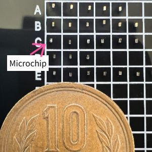
Microchip
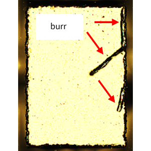
Before deburring
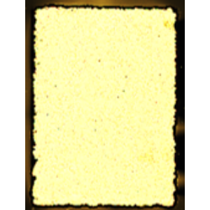
After deburring
- 0.3x0.6mm metallized chip.
- Au burrs with height at the edge.
- Burrs were removed without damage.
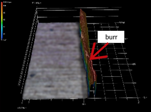
Burr occurrence situation of Cu-based chips
- 1.0x1.0mm Cu-based chip.
- Height burr (right part of the diagram).
- The surface of the material has been blurred due to confidentiality.
- The burrs were too robust to be removed.
- Currently, we are researching the boundaries of removability.
Process and Equipment Introduction
591-4, Ishigaya, Yoshiwa, Ube City, Yamaguchi Prefecture 759-0134
0836-62-1531
Dial your international access code, then 81 for Japan, then 836-62-1531 while omitting the leading ‘0’.

